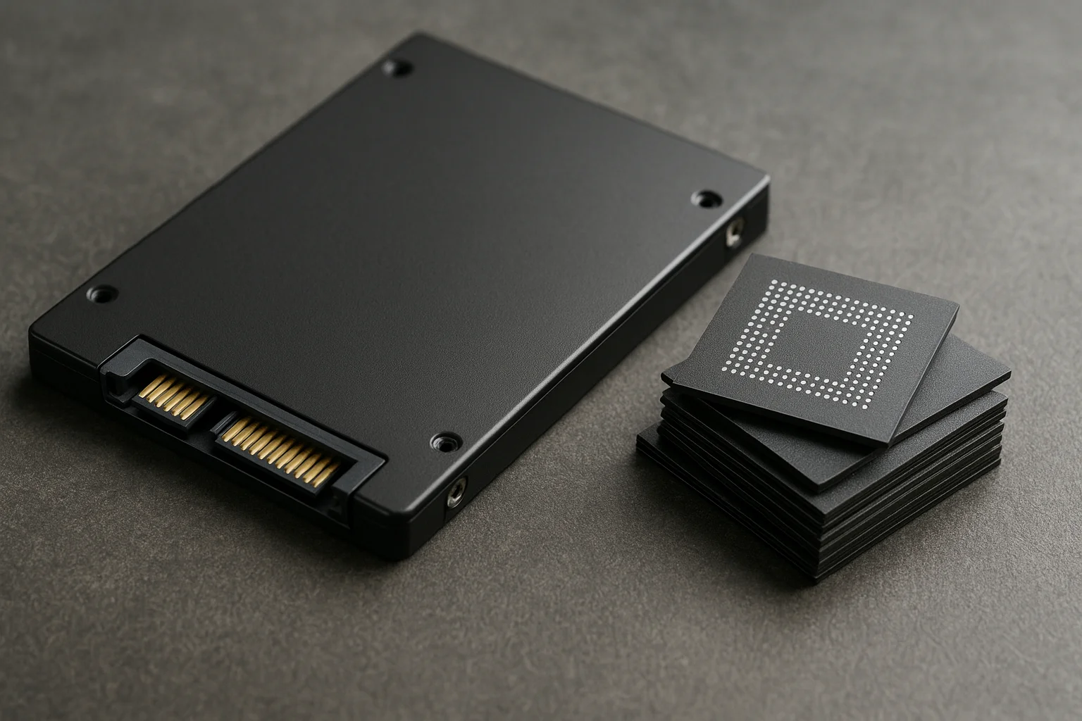
How 500+ Layer 3D NAND Is Changing Density and Scalability
Moving to 500+ layers in 3D NAND represents a major leap in vertical scaling compared with earlier generations (128, 256, 512 logical layers, depending on vendor naming). The most immediate effect is raw bit density: stacking many more layers on the same die footprint multiplies capacity without requiring smaller lithography. For SSD designers and system integrators, that means higher-capacity drives in the same M.2, U.2, or PCIe form factors and a lower cost per gigabyte over time.
Practically, this shift impacts product planning and inventory: manufacturers can offer higher-capacity SKUs without redesigning controllers or PCBs. For data centers, denser chips enable fewer drives per usable capacity target, which can reduce rack space, power draw per gigabyte, and cooling requirements when optimized correctly. However, higher density also amplifies variations in yield and fault isolation, so product teams must plan for stronger error management and spare capacity management in firmware.
Impact on SSD Performance: Speed, Latency, and Endurance
Higher layer counts do not automatically equal faster raw performance. In fact, stacking more layers typically increases internal string lengths and the complexity of charge movement, which can change programming and read latencies. That said, modern controllers and channel architectures mitigate much of this through advanced parallelism, more powerful ECC, and improved firmware algorithms.
Key performance considerations to address when adopting 500+ layer NAND:
- Channel and die-level parallelism - use multiple channels and interleaving to hide per-die latency.
- Stronger ECC and signal processing - plan for higher LDPC overhead and potential increases in ECC decode time.
- Write amplification and garbage collection tuning - deeper stacks can affect block erosion patterns; firmware should adapt erase cycles and placement strategies.
Concrete actions for engineers: benchmark candidate NAND under mixed workload patterns (random small I/O, large sequential writes, sustained write-heavy workloads) and collect metrics on throughput, IOPS, and 99th-percentile latency. Tune firmware GC thresholds and over-provisioning to balance endurance vs. usable capacity.
Manufacturing Challenges Behind Ultra-High-Layer NAND
Producing 500+ layers creates substantial process complexity. Vertical etch uniformity, deposition control, and alignment over hundreds of layers push the limits of current fabrication tools. The main challenges are:
- - Etch aspect ratio: creating tall, narrow holes through hundreds of layers without breakage or variation.
- - Layer-to-layer defect control: a defect in one layer can affect many cells; yield management becomes more granular.
- - Metrology and inspection: new inspection steps and in-line metrology are required to detect sub-nanometer variations across many layers.
From a supply-chain standpoint, expect initial shipments to be limited and priced at a premium until yields improve. For product managers, a practical mitigation strategy is to qualify devices from multiple foundries or fabs where possible, and to build flexible BOMs that allow SKU adjustments as yields and pricing evolve.
Power Efficiency and Thermal Behavior in Next-Gen SSDs
Denser NAND can improve energy efficiency per stored bit, but it also concentrates heat generation. Program/erase cycles and read operations produce thermal hotspots at the die level that, if unmanaged, can accelerate retention loss or increase error rates. System designers should therefore:
- Measure drive-level thermal response under real workloads and identify any throttling or contention points.
- Adjust thermal throttling policies in firmware to avoid abrupt performance drops while protecting endurance.
- Design cooling at the system level (heatsinks, airflow, chassis placement) for sustained workloads rather than peak bursts only.
Example best practice: implement dynamic power modes in firmware that reduce peak program current during sustained writes while increasing parallelism in idle periods to reclaim throughput. Also, monitor SMART thermal metrics to drive host-side placement decisions (for instance, avoiding placing write-heavy VMs on already-hot drives).
Future Consumer and Enterprise Use Cases Enabled by 500+ Layers
Greater capacity per drive unlocks concrete benefits across markets. For consumers, expect high-capacity NVMe drives for gaming and content creation at more affordable price points, enabling single-drive workstations that previously required multi-drive setups. For enterprises and cloud providers, density lowers the number of drives required for a given capacity tier, which simplifies maintenance and reduces rack-level complexity.
Practical deployment scenarios and recommendations:
- - Content delivery and media servers: use higher-capacity drives to consolidate datasets and reduce network dependencies.
- - Edge computing: high-capacity, small-form-factor SSDs simplify deployment at remote sites where physical space is constrained.
- - Tiered storage: pair ultra-dense NAND-based SSDs as nearline tiers for warm data, while keeping hottest data on high-endurance media or caching layers.
When planning migrations or refresh cycles, operators should run capacity vs. performance models rather than assuming denser equals faster. Include endurance budgeting (drive writes per day), rebuild times, and rebuild impact on performance in those models. Finally, keep an eye on firmware upgrade paths: as 500+ layer devices mature, vendors will release controller/firmware updates that materially affect real-world endurance and performance — having a smooth firmware update process is essential.
Comparative snapshot: earlier generations vs 500+ layers
Below is a concise table comparing practical device-level implications across representative layer milestones to help teams make tactical decisions. Use it as a quick reference when selecting SKUs or planning capacity upgrades.
| Characteristic | ~128-256 Layers | ~500+ Layers |
|---|---|---|
| Typical capacity per die | Low to medium | High |
| Power per stored GB | Higher | Lower (but peak thermal spots) |
| Manufacturing yield risk | Lower | Higher initially |
| Firmware complexity | Moderate | Higher (more ECC and management) |
| Best use cases | Performance-sensitive, moderate capacity | High-capacity consolidation, nearline, consumer high-capacity |