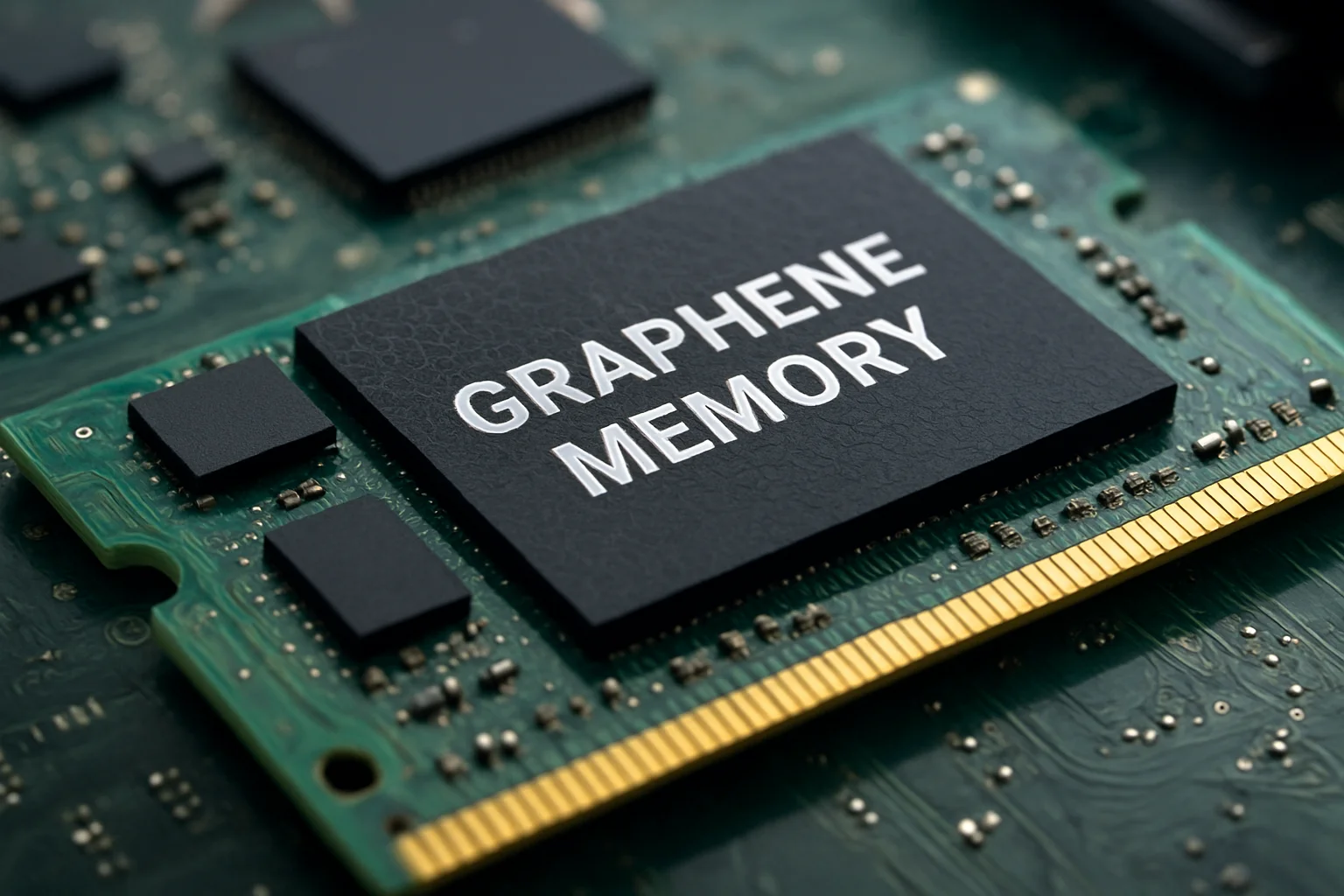
Why Graphene Continues to Captivate the Memory Industry
Graphene keeps attracting attention because it offers a rare combination of properties that are relevant to memory technology: very high electrical conductivity, extreme thinness (one atom thick in ideal form), exceptional mechanical strength, and strong thermal conductivity. These traits make graphene a promising component for next-generation memory cells where switching speed, energy efficiency, and scaling are priorities. For engineers and product managers, the appeal is practical: replacing or supplementing traditional materials with graphene can reduce switching energy, improve heat dissipation in dense arrays, and enable novel device architectures such as atomically thin electrodes or barriers.
Examples of practical motivations include accelerating nonvolatile memory writes with lower voltage, creating flexible memory for wearable devices, and enabling 3D stacking with improved thermal pathways. However, translating intrinsic material advantages into mass-produced memory chips requires addressing manufacturing consistency, integration with existing CMOS processes, and supply-chain maturity. Readers who work in R&D should evaluate graphene not as a miracle material but as a set of engineered tradeoffs to be integrated into proven fabrication flows.
Separating Scientific Breakthroughs from Marketing Hype
Many announcements mix fundamental lab results with product claims. To judge validity, separate these categories:
- Lab breakthrough: A reproducible experiment showing an improved metric (for example, faster switching in a test device under controlled conditions).
- Prototype demonstration: A small-scale device or array that integrates the material but may still rely on special processing or substrates.
- Commercialization claim: Statements about imminent production readiness, cost targets, or compatibility with existing fabrication lines.
Before committing resources, request or verify specific technical details rather than marketing summaries. Useful things to ask or check:
- What is the sample size and device yield reported?
- Are test devices fabricated on industry-standard wafers, or on bespoke substrates?
- Has the material and process been demonstrated at wafer scale or only at the micron level?
- What are endurance, retention, and error rates under realistic environmental conditions?
These questions help distinguish a promising scientific result from a claim that will not survive the demands of high-volume manufacturing. In practice, many promising graphene experiments remain at lab scale because of reproducibility and integration challenges.
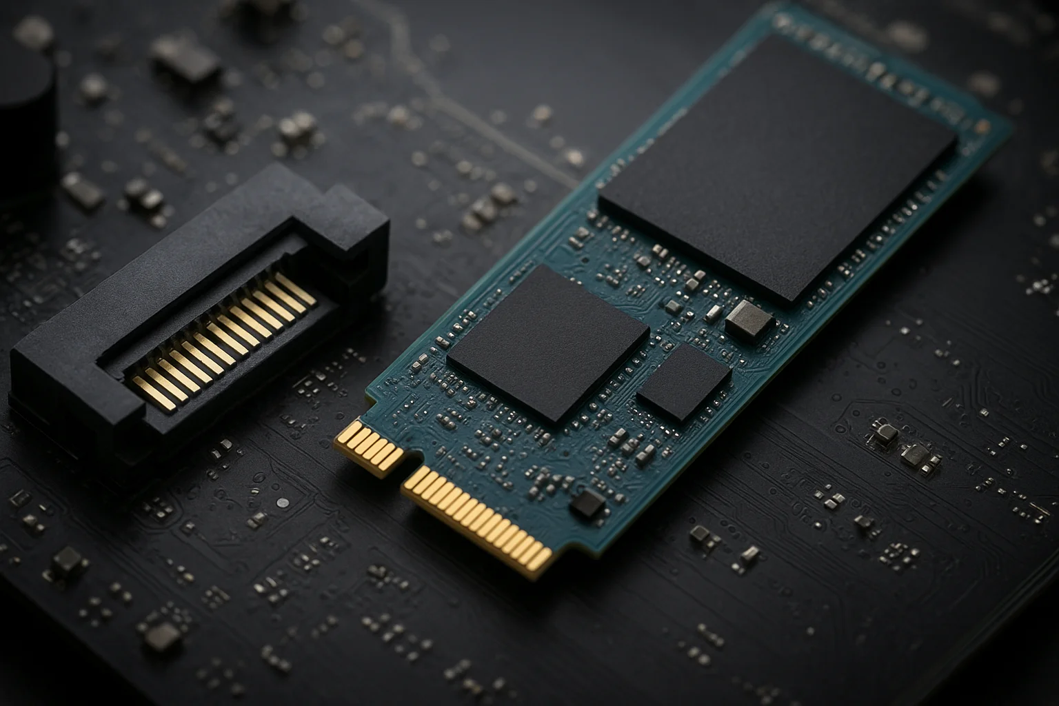
The Current State of Graphene Memory Prototypes and Performance
At present, graphene-enhanced memory research typically appears in two broad device classes:
- Graphene used as an electrode or contact to improve switching speed and reduce contact resistance.
- Graphene or graphene-oxide layers used as part of resistive switching or tunneling stacks to tune switching thresholds and reliability.
Below is a compact comparison that synthesizes common prototype metrics and the realistic expectations for near-term performance. This table is intended to help technical readers weigh tradeoffs when evaluating published results or vendor datasheets.
| Aspect | Typical Prototype Result | Commercial Readiness Note |
|---|---|---|
| Switching energy | Lower by factor of 2 to 10 in some lab devices | Depends on integration; gains shrink when added process steps required |
| Endurance (write cycles) | Ranges widely; some reports show >10^6, many are lower | Needs validation under full-stack operating conditions |
| Retention | Promising in certain resistive designs | Long-term retention tests (years) usually absent |
| Fabrication scale | Mostly small-area devices, parts of wafers | Wafer-scale uniformity is the main bottleneck |
Practically, if you are planning product roadmaps, treat current graphene memory devices as research prototypes that demonstrate potential performance ceilings rather than shipping products. Plan for multi-year maturation before uptake in mainstream SSDs or embedded memory.
Startups Pushing the Boundaries of Graphene-Based Storage
Several startups focus on turning graphene advantages into usable memory modules. Their work typically falls into three strategic approaches:
- Integrating graphene into specific device layers to improve a single metric, for example contact resistance, while leaving the rest of the stack conventional.
- Developing entirely new resistive or tunneling memory architectures where graphene is a core functional element.
- Building wafer-level processes and supply chains for consistent graphene films compatible with foundry flows.
When scouting startups for collaboration or investment, evaluate these operational signals:
- Have they demonstrated devices on industry-standard wafers (150 mm or 300 mm)?
- Do they have partnerships with established fabs or materials suppliers?
- Are their claims backed by independent benchmarking or peer-reviewed publications?
- What is their path to yield improvement and cost per die comparable to incumbent memory technologies?
Actionable advice for engineers: ask for detailed process control documents and sample wafers for independent testing if you are considering integrating a startup's tech into your product line. For investors, focus on teams that combine materials science expertise with semiconductor process engineering and foundry relationships.
Key Challenges Ahead and What to Expect in the Coming Years
Realistic adoption of graphene in memory will hinge on solving four concrete challenges: reproducible large-area synthesis, integration with CMOS back-end-of-line, stable device physics under realistic operating cycles, and a cost model competitive with mature memories. Below are practical expectations and recommended actions for stakeholders.
- For R&D managers - Prioritize reproducibility studies and cross-validation across multiple labs. Insist on long-term cycling and thermal stress tests before scaling.
- For product teams - Build feature roadmaps that treat graphene-enabled improvements as optional value-adds rather than mandatory dependencies. Prepare fallback designs with traditional materials.
- For investors - Look for startups with clear go-to-market plans, foundry partners, and defensible IP that covers process integration, not only device physics.
- For integrators and OEMs - Run pilot programs focused on niche markets where graphene's unique strengths matter, such as flexible electronics, harsh-environment sensors, or ultra-low-power embedded memory.
In the near term (1 to 3 years), expect incremental product demonstrations and selective integration in specialized devices. Over a longer horizon (3 to 7 years), if wafer-scale manufacturing and CMOS compatibility are resolved, graphene elements could appear in hybrid devices that complement rather than replace mainstream memory technologies.
To stay practical and prepared, maintain a small cross-functional team to track validated breakthroughs, maintain relationships with credible startups and foundries, and run reproducible benchmark tests that measure real-world metrics such as energy per write, retention after temperature cycling, and manufacturing yield.